
پرونده:MicroChipAtomicTrap00.jpg

پروندهٔ اصلی (۸۹۰ × ۹۷۶ پیکسل، اندازهٔ پرونده: ۴۴ کیلوبایت، نوع MIME پرونده: image/jpeg)
این پرونده در ویکیانبار موجود است. محتویات صفحهٔ توصیف آن در زیر نمایش داده میشود. |
| توضیح |
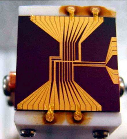
The first microchip atomic trap, designed at the Institute for Laser Science, Japan. The structure of wires is painted with gold at the insulator substrate. The main wire has Z-shape; the magnetic field allows the trapping of neutral atoms due to their magnetic momentum. The ship has sizes 2 x 2 cm. It was placed to the uniform magnetic field (source of this field is not shown in the figure); the traping is realized for so-called "atoms seeking for low magnetic field". The only atoms with positive spin-field energy were trapped. The miminim of the field is realized at the side of the chip, close to the central part of the z-electrode with electric current. This movement is limited by the edges of the "Z". Additional electrodes were designed to allow the play with the effective potential along this wire; the interaction with laser beams and reduction of the trapping potential allow the additional cooling of atoms (coling with vaporation), reaching the BEC. In the current design, the only one additional electrode is supplied with contacts. It was planned to use other electrodes to modify the potential in experiments with single-dimentional quantum mechanics. Actually, more advanced microchip atomic traps were manufactured instead. |
| تاریخ | y.2003 |
| منبع | private communication |
| پدیدآور | Ken-Ichi Nakagawa |
| اجازهنامه (استفادهٔ مجدد از این پرونده) |
copuleft directly from author |
| دیگر نسخهها |
Up to my knowkedge, it is the best resolution image of the First Microship Atomic Trap, ever posted. lower resolution pics are available at
|

|
دارندهٔ حقتکثیر این پرونده به هر کسی اجازهٔ استفاده از آن را به هر منظوری میدهد، به شرط آنکه به شکلی مناسب به دارندهٔ حقتکثیر نسبت داده شود. توزیع مجدد، آثار مشتقشده، استفادهٔ تجاری، و تمام استفادههای دیگر مجاز است. |
|
|
Links
تاریخچهٔ پرونده
روی تاریخ/زمانها کلیک کنید تا نسخهٔ مربوط به آن هنگام را ببینید.
| تاریخ/زمان | بندانگشتی | ابعاد | کاربر | توضیح | |
|---|---|---|---|---|---|
| کنونی | ۱۲ سپتامبر ۲۰۰۷، ساعت ۰۳:۴۷ | | ۸۹۰ در ۹۷۶ (۴۴ کیلوبایت) | Domitori | {{Information |Description=The first microchip atomic trap, designed at Institute for Laser Science, Japan. The main wire has Z-shape; the magnetic field allows the trapping of neutral atoms due t |
کاربرد پرونده
صفحهٔ زیر از این تصویر استفاده میکند:
کاربرد سراسری پرونده
ویکیهای دیگر زیر از این پرونده استفاده میکنند:
- کاربرد در en.wikipedia.org
- کاربرد در es.wikipedia.org
- کاربرد در fr.wikipedia.org
- کاربرد در he.wikipedia.org
- کاربرد در hr.wikipedia.org
- کاربرد در it.wikipedia.org